Cost-efficient laser system for large-area nano and micro structuring processes
Structures in micro and submicro scale are quickly growing application fields. Scientists of the Fraunhofer IWS have developed a unique solution for the fabrication of these structures. For the very first time, our scientists have a technology at their disposal, which allows for the structuring of areas up to 500 x 500 mm² in only a few minutes. The Fraunhofer IWS will present its novel compact system for metal micro structuring processes and surface functionalization at the “Lasermesse LASYS” Stuttgart. The compact system can be adjusted to precisely meet individual customer’s requirements and can be used for the fabrication of arrays with structure widths from 150 nm to 20 µm.


The IWS scientists apply the direct laser interference patterning (DLIP) technique for large area micro structuring and functionalization processes. This technique allows for large area and maskless lithography to fabricate complex structures within one step. (Fig. 1) Conventional structuring technologies are either to slow (sequential procedure) or not flexible enough (mask technique).
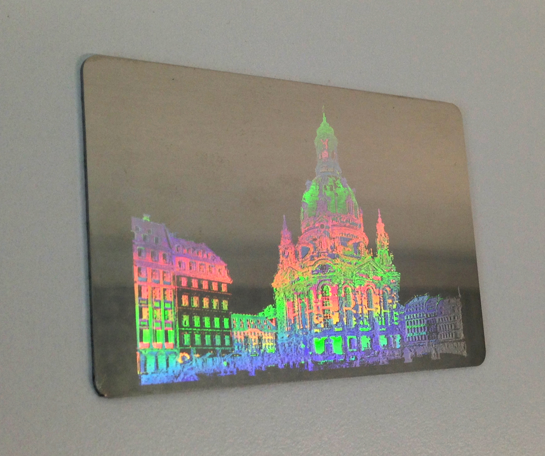
The direct laser interference patterning technology enables the fabrication of 2-, 2.5- and 3-dimensional micro structures on surfaces of both simple and complex compound geometries. To generate the interference structure two or three coherent laser beams of a pulsed laser overlap on plane resp. curved surfaces. In the generated intensities maxima of the light waves the material is locally ablated or modified via controllable process parameters such as pulse energy and wavelength. Thus electric, chemical and/or mechanical properties of polymer surfaces, metals, ceramics and single-/multi-layers can be periodically varied. Furthermore, the IWS developed system allows for the local variation of structure widths and thus for the generation of holographic structures directly on metal. (Fig. 2)
Depending on which material and structure topography is used, the IWS method makes novel applications in the field of automotive and medical industries feasible and affordable. We will present selected examples at the LASYS in Stuttgart.
Discover for yourself the efficiency of our novel system. You are cordially invited to visit us at the Fraunhofer booth, hall 4, booth C31 at the LASYS 2014 and feel free to contact our experts.
 Fraunhofer Institute for Material and Beam Technology IWS