MSD process for the coating of Mo/Si multilayers

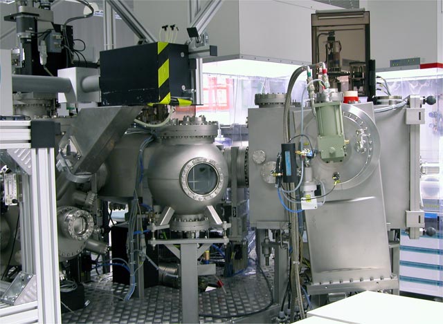
UHV clustertool for generating precision nanometer multilayer systems

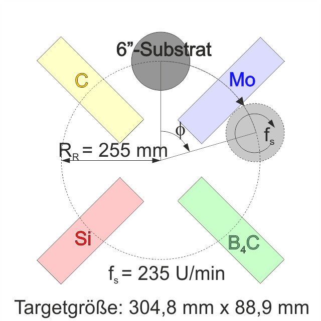
Schematic diagram of the target-substrate arrangement
Layer fabrication
- plasma generation by impact ionization
- static magnetic field to increase the plasma density
- sputtering of the target by impact processes between sputter gas ions and target atoms
- condensation of the sputtered particles on the substrate surface
Process conditions
- vacuum: p ~ 2 x 10⁻⁸ mbar
- Ar sputter gas pressure: p > 7 x 10⁻⁴ mbar
- magnetron operation: DC, RF for reactive processes
- number of sputtering sources: 4
- discharge power: > 1 kW
- target size: 304,8 mm x 88,9 mm (12'' x 3,5'')
- substrate size: load-lock up to a diameter of 200 mm, larger substrates of up to 500 mm have to be operated by hand through the chamber door
- target-substrate distance: 50 ... 100 mm
Advantages of the MSD procedure
- high coating rates
- very stable, simple and reproducible process operation
- excellent film homogeneity
- simple scalability to larger geometries
Applications
- EUV reflection layer (Mo/Si)
- X-ray optical multilayer systems (W/Si, W/B4C, Mo/B4C, ...)
- XUV reflection layers (Cr/Sc, Sc/Si, Mo/Si, ...)
- monochromators for X-ray fluorescence analysis (W/Si, W/B4C, Mo/Si, Mo/B4C, Cr/Sc, Cr/C, ...)
- metallic coatings for reflections (Al, Ag, ...)
- dielectic multilayer systems (SiO2/Al2O3, SiO2/TiO2, ...)
- layer thickness standards (Ru, Cu, Al, Ti, Cr, Si, C, B4C, Sc, Ag, ...)
 Fraunhofer Institute for Material and Beam Technology IWS