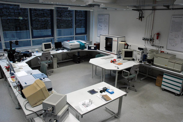
The sensitive determination of the surface condition is an essential component in all those cases, in which the precise surface design is decisive, that means, especially in the photovoltaic and semi-conducting industry.
Fraunhofer IWS engineers employ optical spectroscopic analysis methods ranging from ultra violet to ultra red spectrum. These non-invasive methods are very suitable for various materials, such as ceramics, semi-conductors, glass, polymers, metals or thin film systems.
Our offer comprises the film detection and analysis, surface characterizations (impurities) as well as the determination of humidity, composition, functionalization and material structure. Thin film systems can be additionally investigated with respect to their optical function (refraction index, extinction coefficient), their film thickness (nm to µm), the film structure and inhomogeneities. Furthermore, we have different testing systems to determine the photocatalytical activity at our disposal.
 Fraunhofer Institute for Material and Beam Technology IWS