 Fraunhofer Institute for Material and Beam Technology IWS
Low-Cost Laser Process Technology for Large-Area Micro/Nano-Fabrication
Given the need for more highly functional materials, complex surface structures with features in the micron or submicron length scales have become increasingly important. In order to reduce costs for the fabrication of these micro/sub-micrometer structures over large areas, a new system has been developed at Fraunhofer IWS in Dresden. For the first time, this system enables to produce micropatterns at speeds up to several square centimeters within a few seconds. At the World of Photonics 2011 exposition in Munich, the Fraunhofer IWS will present a compact and versatile system for micro-structuring as well as functionalization of surfaces for all types of materials, including metals, ceramics and polymers. The system can be adapted according to the customer’s requirements to fabricate micro arrays with structures ranging from 180 nm to 20 µm at speeds of approximately 1 to 100 cm²/s.
")
Fraunhofer IWS Dresden uses the Direct Laser Interference Patterning (DLIP) method for the large-area fabrication of microstructures as well as the functionalization of surfaces. Unlike many other traditional lithography techniques that are either too slow or inflexible, DLIP is a one-step process and does not require any photo masks or templates to generate a surface pattern on large areas (Fig. 1).
Direct Laser Interference Patterning allows the fabrication of 2-, 2.5- and 3-dimensonal micro-structures on components with simple as well as complex geometry. To generate a periodic structure, N collimated and coherent beams of a q-switched Nd:YAG laser are overlapped on a planar or non-planar surface. By adopting the proper processing parameters, such energy den-sity or wavelength, the surface of different materials can be locally ablated or modified at the interference maxima positions, and thus generating a periodic pattern. Moreover, also the elec-trical, chemical and/or mechanical surface properties of polymers, metals, ceramics and coatings can be periodically varied.
Based on the material and the required surface topography, DLIP could potentially be deployed for several promising applications within the automotive industry and life science. Some examples are shown below.
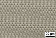
 Patterned titanium Surface Photo: Fraunhofer IWS Dresden |
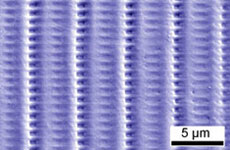
 Patterned stainless steel Photo: Fraunhofer IWS Dresden |
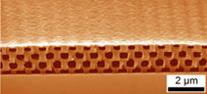 Micro channels in a photo resist with high aspect ratio Photo: Fraunhofer IWS Dresden |
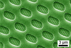 Biologically-inspired artificial structure (Diatomee C. Walesi) Photo: Fraunhofer IWS Dresden |