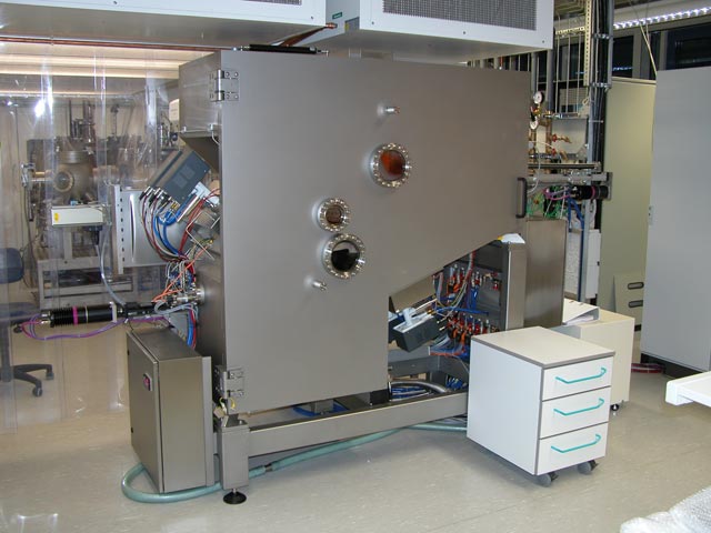
UHV ion beam sputtering system for nanometer precise coatings and etching procedures

UHV ion beam sputtering system for nanometer precise coatings and etching procedures

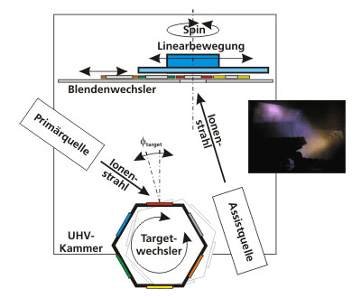
Arrangement of ion source, targets and substrate in the ion beam sputtering system
Technical data
- vacuum:
- process chamber: p < 2·10-8 mbar
- load lock: p < 5·10-7 mbar
- substrate:
- round up to Ø = 200 mm
- square to L = 500 mm (without spin)
- targets: 6 pieces, size: 400 x 200 mm2
- ion beam sources:
- primary source for target sputtering
- secondary source for assisting and etching operation
- activation: ECR (electrode cyclotron resonance)
- size: 400 x 100 mm2
- ion energies: E = 50 - 2000 eV
- optics:
- for beam shaping and film thickness homogenization processes
- 4 pieces, automatically exchangeable
Application
- synthesis of nanometer single- and multilayers for X-ray and EUV- optical systems
- synthesis of dielectrical multilayers for laser optical systems
Characteristics
- extremely low micro roughnesses in the range of σrms = 0.15 ... 0.3 nm
- uniformity: 99.0 - 99.9 % over Ø 200 mm
- absorption-free dielectrical coatings within the UV-IR spectral range
 Fraunhofer Institute for Material and Beam Technology IWS